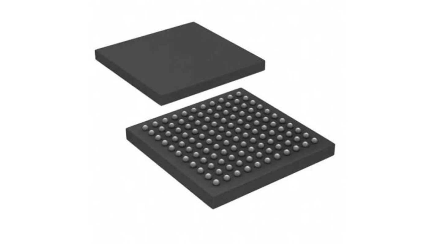
Infineon NOR 64 MB QPI, Parallel, SPI Flash Memory 8-Pin USON, S25FL064LABNFV040
- RS Stock No.:
- 181-8386P
- Mfr. Part No.:
- S25FL064LABNFV040
- Brand:
- Infineon

Unavailable
RS will no longer stock this product.
- RS Stock No.:
- 181-8386P
- Mfr. Part No.:
- S25FL064LABNFV040
- Brand:
- Infineon
Specifications
Technical Reference
Legislation and Compliance
Product Details
Find similar products by selecting one or more attributes.
Select all | Attribute | Value |
|---|---|---|
| Brand | Infineon | |
| Product Type | Flash Memory | |
| Memory Size | 64MB | |
| Interface Type | QPI, Parallel, SPI | |
| Package Type | USON | |
| Pin Count | 8 | |
| Mount Type | Surface | |
| Cell Type | NOR | |
| Maximum Supply Voltage | 3.6V | |
| Minimum Supply Voltage | 2.7V | |
| Minimum Operating Temperature | -40°C | |
| Maximum Operating Temperature | 105°C | |
| Standards/Approvals | RoHS | |
| Length | 4mm | |
| Height | 0.55mm | |
| Number of Bits per Word | 8 | |
| Number of Words | 8K | |
| Series | S25FL064L | |
| Automotive Standard | AEC-Q100 | |
| Select all | ||
|---|---|---|
Brand Infineon | ||
Product Type Flash Memory | ||
Memory Size 64MB | ||
Interface Type QPI, Parallel, SPI | ||
Package Type USON | ||
Pin Count 8 | ||
Mount Type Surface | ||
Cell Type NOR | ||
Maximum Supply Voltage 3.6V | ||
Minimum Supply Voltage 2.7V | ||
Minimum Operating Temperature -40°C | ||
Maximum Operating Temperature 105°C | ||
Standards/Approvals RoHS | ||
Length 4mm | ||
Height 0.55mm | ||
Number of Bits per Word 8 | ||
Number of Words 8K | ||
Series S25FL064L | ||
Automotive Standard AEC-Q100 | ||
The Cypress FL-L Family devices are Flash Nonvolatile Memory products using: Floating Gate technology,65-nm process lithography The FL-L family connects to a host system via a Serial Peripheral Interface (SPI). Traditional SPI single bit serial input and output (Single I/O or SIO) is supported as well as optional two bit (Dual I/O or DIO) and four bit wide Quad I/O (QIO), and Quad Peripheral Interface (QPI) commands. In addition, there are Double Data Rate (DDR) read commands for QIO and QPI that transfer address and read data on both edges of the clock. The architecture features a Page Programming Buffer that allows up to 256-bytes to be programmed in one operation and provides individual 4 KB sector, 32 KB half block sector, 64 KB block sector, or entire chip erase. By using FL-L family devices at the higher clock rates supported, with Quad commands, the instruction read transfer rate can match or exceed traditional parallel interface, asynchronous, NOR Flash memories, while reducing signal count dramatically. The FL-L family products offer high densities coupled with the flexibility and fast performance required by a variety of mobile or embedded applications. Provides an ideal storage solution for systems with limited space, signal connections, and power. These memories offer flexibility and performance well beyond ordinary serial flash devices. They are ideal for code shadowing to RAM, executing code directly (XIP), and storing re-programmable data.
Related links
- Infineon NOR 64 MB QPI SPI Flash Memory 8-Pin USON, S25FL064LABNFV040
- Infineon NOR 64 MB SPI Parallel Flash Memory 8-Pin USON
- Infineon NOR 64 MB SPI Parallel Flash Memory 8-Pin USON, S25FL064LABNFI041
- Infineon NOR 64 MB SPI Flash Memory 8-Pin USON
- Infineon NOR 64 MB SPI Flash Memory 8-Pin USON, S25FL064LABNFI040
- Winbond NOR 2 MB SPI Flash Memory 8-Pin USON
- Winbond NOR 1 MB SPI Flash Memory 8-Pin USON
- Winbond NOR 4 MB SPI Flash Memory 8-Pin USON
