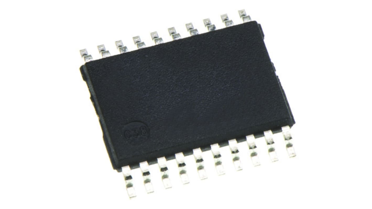
Toshiba 74VHCT573AFT 8bit-Bit Octal D Type Latch, Transparent D Type, 20-Pin TSSOP
- RS Stock No.:
- 171-3540
- Mfr. Part No.:
- 74VHCT573AFT
- Brand:
- Toshiba

Unavailable
RS will no longer stock this product.
- RS Stock No.:
- 171-3540
- Mfr. Part No.:
- 74VHCT573AFT
- Brand:
- Toshiba
Specifications
Technical Reference
Legislation and Compliance
Product Details
Find similar products by selecting one or more attributes.
Select all | Attribute | Value |
|---|---|---|
| Brand | Toshiba | |
| Logic Family | 74VHC | |
| Latch Mode | Transparent | |
| Latching Element | D Type | |
| Number of Elements per Chip | 19 | |
| Number of Bits | 8bit | |
| Number of Channels per Chip | 8 | |
| Polarity | Inverting | |
| Mounting Type | Surface Mount | |
| Package Type | TSSOP | |
| Pin Count | 20 | |
| Dimensions | 6.5 x 4.4 x 1mm | |
| Height | 1mm | |
| Length | 6.5mm | |
| Maximum Operating Supply Voltage | 5.5 V | |
| Maximum Operating Temperature | +125 °C | |
| Automotive Standard | AEC-Q100 | |
| Width | 4.4mm | |
| Minimum Operating Supply Voltage | 4.5 V | |
| Minimum Operating Temperature | -40 °C | |
| Select all | ||
|---|---|---|
Brand Toshiba | ||
Logic Family 74VHC | ||
Latch Mode Transparent | ||
Latching Element D Type | ||
Number of Elements per Chip 19 | ||
Number of Bits 8bit | ||
Number of Channels per Chip 8 | ||
Polarity Inverting | ||
Mounting Type Surface Mount | ||
Package Type TSSOP | ||
Pin Count 20 | ||
Dimensions 6.5 x 4.4 x 1mm | ||
Height 1mm | ||
Length 6.5mm | ||
Maximum Operating Supply Voltage 5.5 V | ||
Maximum Operating Temperature +125 °C | ||
Automotive Standard AEC-Q100 | ||
Width 4.4mm | ||
Minimum Operating Supply Voltage 4.5 V | ||
Minimum Operating Temperature -40 °C | ||
The 74VHCT573A is an advanced high speed CMOS OCTAL LATCH with 3-STATE OUTPUT fabricated with silicon gateC2MOS technology. It achieves the high speed operation similar to equivalent Bipolar Schottky TTL while maintaining the CMOS low power dissipation. This 8-bit D-type latch is controlled by a latch enable input (LE) and an output enable input (OE).When the OE input is high, the eight outputs are in a high impedance state. The input voltage are compatible with TTL output voltage. This device may be used as a level converter for interfacing 3.3V to 5 V system. Input protection and output circuit ensure that 0 to 5.5 V can be applied to the input and output (Note) pins without regard to the supply voltage. These structure prevents device destruction due to mismatched supply and input/output voltages such as battery back up, hot board insertion, etc.
Wide operating temperature range: Topr = -40 to 125
High speed: Propagation delay time = 7.7 ns (typ.) at VCC = 5.0 V
Low power dissipation: ICC = 4.0 μA (max) at Ta = 25
Compatible with TTL inputs: VIL = 0.8 V (max)VIH = 2.0 V (min)
Power down protection is provided on all inputs and outputs.
Balanced propagation delays: tPLH ≈ tPHL
Low noise: VOLP = 1.5 V (max)
Pin and function compatible with the 74 series (74ACT/HCT/AHCT etc.) 573 type.