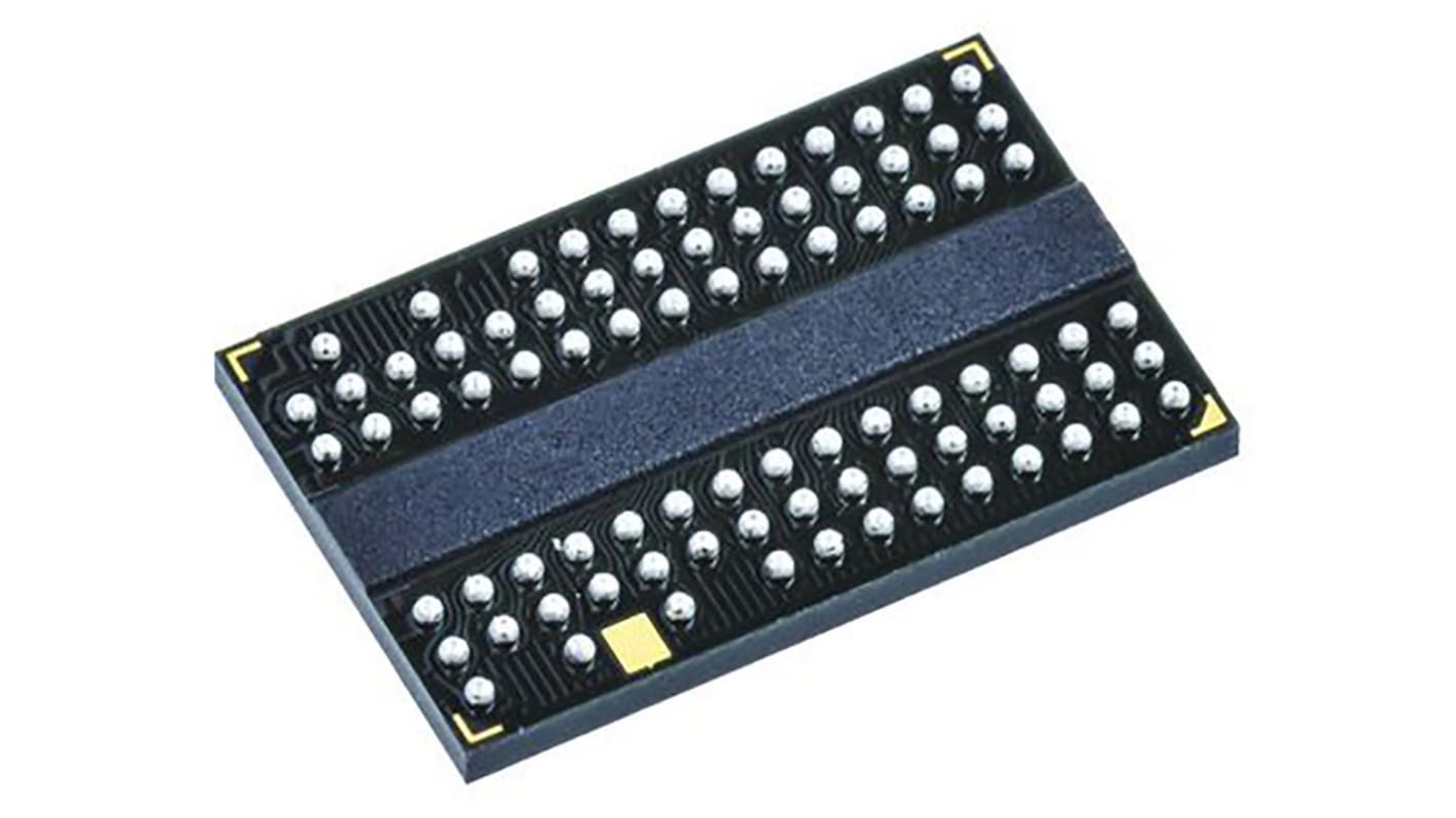
Winbond W972GG6KB25I SDRAM 2 GB Surface, 84-Pin 16 bit WBGA
- RS Stock No.:
- 188-2835
- Mfr. Part No.:
- W972GG6KB25I
- Brand:
- Winbond

Currently unavailable
We don't know if this item will be back in stock, RS intend to remove it from our range soon.
- RS Stock No.:
- 188-2835
- Mfr. Part No.:
- W972GG6KB25I
- Brand:
- Winbond
Specifications
Technical Reference
Legislation and Compliance
Product Details
Find similar products by selecting one or more attributes.
Select all | Attribute | Value |
|---|---|---|
| Brand | Winbond | |
| Product Type | SDRAM | |
| Memory Size | 2GB | |
| Organisation | 256M x 8 bit | |
| Data Bus Width | 16bit | |
| Address Bus Width | 17bit | |
| Number of Bits per Word | 8 | |
| Maximum Clock Frequency | 533MHz | |
| Maximum Random Access Time | 0.4ns | |
| Number of Words | 256M | |
| Mount Type | Surface | |
| Package Type | WBGA | |
| Pin Count | 84 | |
| Minimum Operating Temperature | -40°C | |
| Maximum Operating Temperature | 95°C | |
| Width | 8.1mm | |
| Series | W972GG6KB | |
| Height | 0.6mm | |
| Length | 12.6mm | |
| Standards/Approvals | RoHS | |
| Minimum Supply Voltage | 1.7V | |
| Automotive Standard | No | |
| Maximum Supply Voltage | 1.9V | |
| Supply Current | 280mA | |
| Select all | ||
|---|---|---|
Brand Winbond | ||
Product Type SDRAM | ||
Memory Size 2GB | ||
Organisation 256M x 8 bit | ||
Data Bus Width 16bit | ||
Address Bus Width 17bit | ||
Number of Bits per Word 8 | ||
Maximum Clock Frequency 533MHz | ||
Maximum Random Access Time 0.4ns | ||
Number of Words 256M | ||
Mount Type Surface | ||
Package Type WBGA | ||
Pin Count 84 | ||
Minimum Operating Temperature -40°C | ||
Maximum Operating Temperature 95°C | ||
Width 8.1mm | ||
Series W972GG6KB | ||
Height 0.6mm | ||
Length 12.6mm | ||
Standards/Approvals RoHS | ||
Minimum Supply Voltage 1.7V | ||
Automotive Standard No | ||
Maximum Supply Voltage 1.9V | ||
Supply Current 280mA | ||
The W972GG6KB is a 2G bits DDR2 SDRAM, and speed involving -18, -25/25I, and -3/-3I.
Double Data Rate architecture: two data transfers per clock cycle
CAS Latency: 3, 4, 5, 6 and 7
Burst Length: 4 and 8
Bi-directional, differential data strobes (DQS and /DQS ) are transmitted / received with data
Edge-aligned with Read data and center-aligned with Write data
DLL aligns DQ and DQS transitions with clock
Differential clock inputs (CLK and /CLK)
Data masks (DM) for write data
Commands entered on each positive CLK edge, data and data mask are referenced to both edges of /DQS
Posted /CAS programmable additive latency supported to make command and data bus efficiency
Read Latency = Additive Latency plus CAS Latency (RL = AL + CL)
Off-Chip-Driver impedance adjustment (OCD) and On-Die-Termination (ODT) for better signal quality
Auto-precharge operation for read and write bursts
Auto Refresh and Self Refresh modes
Precharged Power Down and Active Power Down
Write Data Mask
Write Latency = Read Latency - 1 (WL = RL - 1)
Interface: SSTL_18
Related links
- Winbond W972GG6KB25I SDRAM 2 GB Surface, 84-Pin 16 bit WBGA
- Intelligent Memory IM2G16D2DBBG-25I SDRAM 2 GB Surface, 84-Pin 16 bit FBGA-84 Ball
- Alliance Memory SDRAM 2 GB Surface, 84-Pin 16 bit FBGA
- Alliance Memory AS4C128M16D2A-25BCN SDRAM 2 GB Surface, 84-Pin 16 bit FBGA
- Intelligent Memory IM5116D2DDBG-25 SDRAM 2 GB Surface, 84-Pin 16 bit FBGA-84 Ball
- Intelligent Memory IM5116D2DDBG-25I SDRAM 2 GB Surface, 84-Pin 16 bit FBGA-84 Ball
- Alliance Memory AS4C128M16D3LC-12BCNTR SDRAM 2 GB Surface, 96-Pin 16 bit FBGA-96 Ball
- Alliance Memory AS4C128M16MD4-062BAN SDRAM 2 GB Surface, 200-Pin 16 bit 200-Ball TFBGA